


10x10_ProtoBoard_Rev_A.zip
Design by: fmuntean
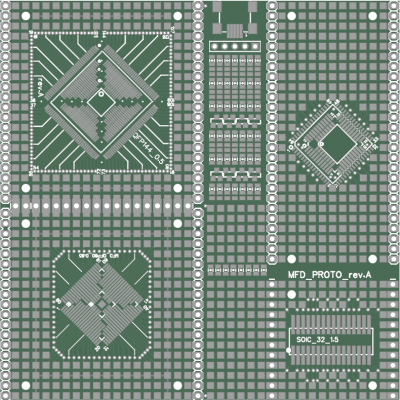
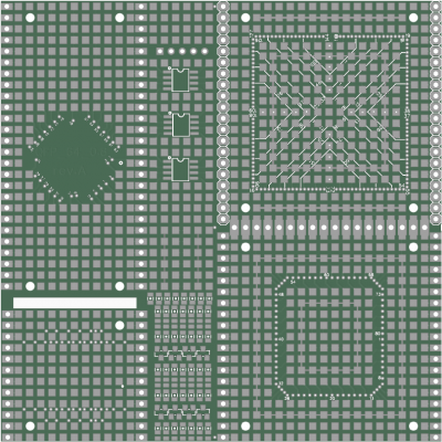
A prototype board for lots of SMD components.
On the internet usually only find QFP or SOIC to DIP adapters where all pins are routed to the border headers. Everybody building circuits know that not all pins are going to be used and that decouplic capacitors are better to be put as closed to the IC as possible.
I designed this boards taking all that in consideration and much more.
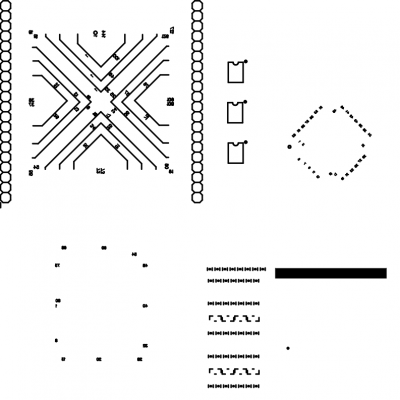
The board is designed based on the standard 100x100mm surface and using two layer design.
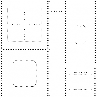
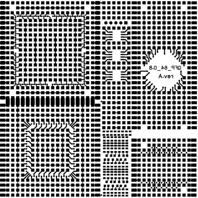
This prototype board has different areas that can accomodate different chips:
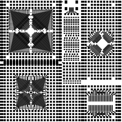
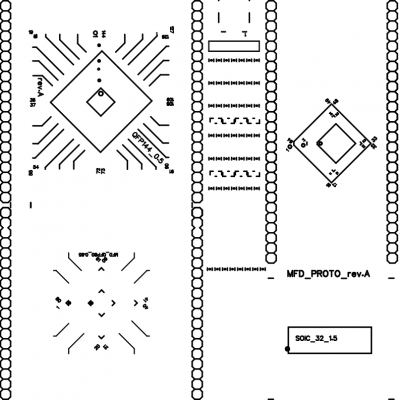
a QFP 32 to 64 0.8mm pitch area with pins wired up to at least one pad.
a QFP 32 to 144 0.5mm pitch area with pins wired up to at least one pad.
a QFP 16 to 80 0.65mm pitch area with pins wired up to at least one pad.
a SOIC 32 1.27mm pitch area with pins wired to the pads.
micro/mini usb connector available on top.
multiple headers single line are mounted in different places on the board. They can be used for connectors or to mount any other dauther card on top of bellow.
some of the traces (which are provided by default) can be cut to fit the schematic as needed.
some of the traces are thinned already to help with applying more solder if they are used as ground. They are kept thin enough in order to allow for cutting if needed.
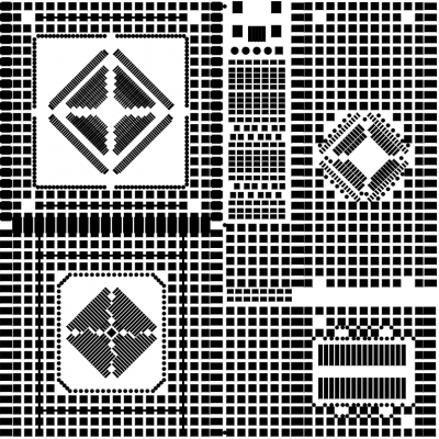
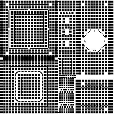
a small area for transistors or any small SOT-3 ICs
a small area supporting 3 SOIC-8 ICs.
lots of pads for soldering pasive components as: SMD resistors, capacitors, diodes, etc.
the pads are extended to the edges to allow for soldering of dual line header connectors.
And that is not all. If your project is not big enough to use the entire area then look for small holes/vias that I put in specific places which will allow you to easily score and cut the board in smaller and still usable proto boards.
If your project do not fit on this board then use two of them and stack them up. There is a reason why the IC pins are not wired directly to any of the trough hole pads.
There is still more I can talk about this board capabilities and as this is meant as a prototype board use your imagination and make it yours.
I would only say just this last tip: the vias are thinned for a reason; so you can solder AWG30 wrapping wire and you will find them very usefull when testing the soldering of the ICs on the board.